


认证信息
认 证:工商信息已核实
访问量:982781
手机网站
扫一扫,手机访问更轻松
产品分类
公司品牌
品牌传达企业理念
产品简介
产品详情
AZ 1500 Series Standard Photoresists
GENERAL INFORMATION
This series of positive photoresists actually consists of three different products. They all contain the same photoactive compound (PAC) which responds to the whole UV-spectrum from 310 - 440 nm covering the three main mercury lines, i, h and g. They may be used with broadband as well as monochromatic exposure. Different novolak resins or fractions thereof were chosen to adopt them for different demands, this is indicated by a corresponding suffix of the product designation:
AZ 1500 (no suffix) is the most popular family and a direct safer solvent (PGMEA) substitute for AZ 1370, AZ 1470 , AZ 1350J, AZ 1450J, AZ 1375. It is available in different viscosities to cover the coating thickness range from 0.5 to 4.0 μm. Due to the slightly lower evaporation rate of the PGMEA(compared to cellosolve acetate based solvent system) these resists will show about 5 - 10% higher photospeed which may be compensated by increasing prebake temperature about 5°C. This resists may be used for wet- and dry-etch and cover all demands for general semiconductor manufacturing and other applications with resolution down to 1 μm.
AZ 1514 H is the safer solvent substitute for the well known AZ 1350 H which is now almost 25years old and intended for contact and proximity printing. For this application a low photospeed for better control of exposure (about 10s at 15 mW/cm2) and thus a forgiving resist is the best choice. For many years the "non safe solvent" counterparts AZ 111 S and AZ 1350 H have been the standard resists for making semiconductors, AZ 111 S for wet-etch of oxides, AZ 1350 H for aluminium and nitride etch.
AZ 1500 HS family was developed in 1990. The background for this development was the fact that in making discrete and bipolar semiconductor devices wet-etching is still very common. For wet-etching adhesion is the most important issue. Especially on aluminium the mousebite-phenomenon is well known. To solve this problem we have chosen a low molecular weight novolak resin fraction resulting in significantly improved adhesion and also very high photospeed (therefore the suffix High Speed). Meanwhile AZ 1500 HS has proven its superior performance in several production lines and lead to less rework and higher yields.
All AZ 1500-series resists are compatible with all common developers used for positive photoresists, like AZ 351B (diluted 1:4), 0.5% NaOH solution and metal ion free developers like AZ 726MIF. While AZ 1500-family and AZ 1514H are optimised for best process latitude at 50 - 60 seconds development time, AZ 1500HS-family performs best at 20 - 30 seconds development time resulting in a high throughput lithographic process.
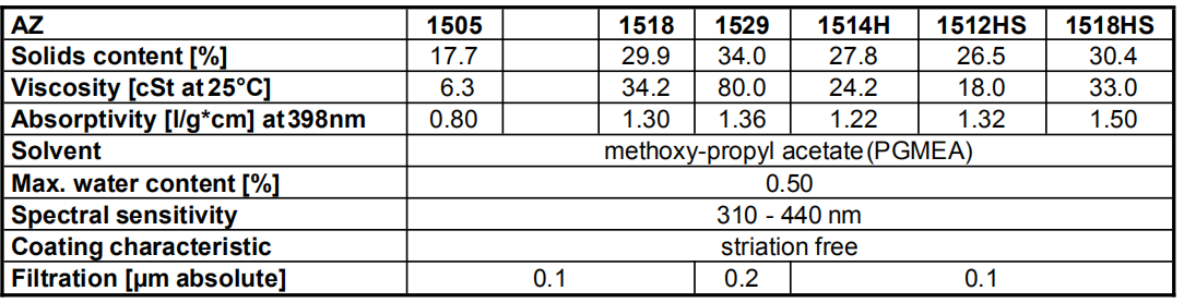
PHYSICAL and CHEMICAL PROPERTIES
FILM THICKNESS [μm] as FUNCTION of SPIN SPEED (characteristically)
PROCESSING GUIDELINES
HANDLING ADVISES
Consult the Material Safety Data Sheets provided by us or your local agent!
This AZ Photoresists are made up with our patented safer solvent PGMEA. They are flammable liquids and should be kept away from oxidants, sparks and openflames.
Protect from light and heat and store in sealed original containers between 0°C and 25°C, exceeding this range to -5°C or +30°C for 1 week does not adversely affect the properties.
Shelf life is limited and depends on the resist series. The expiration date is printed on the label of every bottle below the batch number and coded as [year/month/day].
AZ Photoresists are compatible with most commercially available wafer processing equipment.
Recommended materials include PTFE, stainless steel and high-density poly-ethylene and -propylene.
- 推荐产品
- 供应产品
- 产品分类
- 德Optosol-K3太阳能吸收率发射率检测仪
- N-TEC全自动晶圆贴片机BW 228-5FA
- N-TEC全自动晶圆贴片压合机228-3FA
- N-TEC全自动晶圆清洗机BW 232FA
- 半导体测试探针台KUP007,EMP100C,EMP100B,EMP50S
- 日本JEOL截面样品制备装置IB-19520CCP
- 英国Denton高真空蒸发器平台DV-502B
- 德国laVision BioTec光片照明显微镜Ultramicroscop
- 芬兰PICOSUN原子层沉积机P-300S Pro ALD
- 德国Sentech等离子体增强原子层沉积机PE-ALD
- PICOSUN P-200S Pro ALD生产型原子层沉积机
- 英国HHV真空镀膜系统Auto500 GB
- P-1000 Pro ALD芬兰PICOSUN生产型原子层沉积机
- 日本JEOL核磁共振谱仪JNM-ECZR系列
- 德国Neaspec太赫兹近场光学显微镜THz-NeaSNOM-30nm
- 芬兰PICOSUN标准型原子层沉积机R-200