


认 证:工商信息已核实
访问量:992466
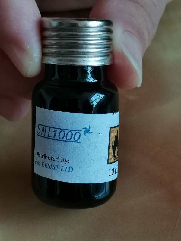
SML Resist – Product Information
Introduction
The hardware of electron beam lithography has improved continuously over the past few decades,but electron beam resist technology has not, and this is now one of the main limiting factors in improved EBL performance.
The high performance SML resist is a novel polymer that has been specifically designed to answer the demands of the EBL community. It can be simultaneously patterned into high resolution and high aspect ratio patterns, even at low acceleration voltages, and without the aid of proximity effect correction.
Processing
Other Processing Information
。 Slow dry etch rate: significantly slower than PMMA
。 Can be hard-baked: Tg=109℃
。 Can be re-exposed after development
。 Other developers such as IPA:H2O can also be used
。 Shelf life is guaranteed for 6 months
Products – Spin Curves
How it Works - Monte Carlo Simulations
The following Monte Carlo simulations compare the electron scattering behaviour of PMMA and SML resists at 30KeV and at 100KeV. Each simulation contains 500 incident electrons and created secondary electrons are shown in light blue.
Comparison of 50nm thick PMMA & SML on Si substrate exposed @30keV
These simulations show that at both 30KeV and 100KeV:
。 The lateral scattering of incident electrons is much less in SML than in PMMA
。The number of secondary electrons created is much less in SML than in PMMA
These properties mean that SML resist is less susceptible to the problem of proximity effect and enables the patterning of features with smaller critical dimensions, larger aspect ratio, and straighter side-walls, than those obtainable in PMMA resist.
About EM Resist Ltd
EM Resist Ltd specialises in electron beam lithography resists and applications. We develop and manufacture electron beam resists in a purpose built cleanroom facility to ensure maximum quality and performance. We also have a dedicated team of applications scientists to aid our customers with their questions and requirements.
Our products and expertise are the result of many years research by experienced physicists and material scientists in both academia and industry. We are based in Macclesfield, UK and have global sales and distribution channels for our products.
SML Resist – Processing Information
Introduction
SML resist has been specifically designed for electron beam lithography. It is a polymer material and can be processed in exactly the same way as other polymer resists such as PMMA or ZEP.
Storage
Do not refrigerate.
Store at room temperature.
Store away from direct sunlight and ignition sources.
The shelf life is guaranteed for six months.
Typical Processing Conditions
The processes outlined below are our standard processes. Other common resist processes can also be used.
Substrate Preparation:
Solvent clean with Acetone and IPA.
SML has excellent adhesion to most substrates so HMDS is not generally required.
Spin Coating:
See spin curves below.
Baking:
Hot plate @ 180 C for 120-180 seconds.
Exposure:
Development:
MIBK:IPA (1:3) for 30 seconds, followed by a rinse in IPA for 15 seconds.
Hard-Bake:
Convection oven @ 80 C for 30 minutes. (Tg=109℃ )
Remover:
Acetone.
Spin Curves
Spin coater settings:
。Ramp up time = 5 seconds.
。Spin time = 20 seconds.
。Ramp down time = 10 seconds.
Safe Handling and Disposal
Caution: Flammable liquid.
Open in a well ventilated area.
Avoid inhalation.
Avoid direct contact with skin and eyes.
Wear appropriate safety equipment such as glasses and gloves.
In case of direct contact with eyes, rinse thoroughly with water and seek medical advice.
Read the Material Safety Data Sheet.
Dispose of in appropriate waste containers for non-halogenated waste.
About EM Resist Ltd
EM Resist Ltd specialises in electron beam lithography resists and applications. We develop and manufacture electron beam resists in a purpose built cleanroom facility to ensure maximum
quality and performance. We also have a dedicated team of applications scientists to aid our
customers with their questions and requirements.
Our products and expertise are the result of many years research by experienced physicists and
material scientists in both academia and industry. We are based in Macclesfield, UK and have
global sales and distribution channels for our products.
100 KeV Exposure Parameters
Please note that the best results (aspect ratio and resolution) are generally achieved when a relatively low beam current is used.
100 KeV Exposure Parameters
30 KeV Exposure Parameters
25 KeV Exposure Parameters
SML Resist – Contrast & Sensitivity
SML – A Complete Solution for you – Part 1 / 2
E M Resist can offer two complete solutions to suit your distribution needs in your territory.
SML – A Complete Solution for you – Part 2 / 2
- 推荐产品
- 供应产品
- 产品分类
- 德Optosol-K3太阳能吸收率发射率检测仪
- N-TEC全自动晶圆贴片机BW 228-5FA
- N-TEC全自动晶圆清洗机BW 232FA
- N-TEC全自动晶圆贴片压合机228-3FA
- 半导体测试探针台KUP007,EMP100C,EMP100B,EMP50S
- 日本JEOL截面样品制备装置IB-19520CCP
- 英国Denton高真空蒸发器平台DV-502B
- 德国laVision BioTec光片照明显微镜Ultramicroscop
- 芬兰PICOSUN原子层沉积机P-300S Pro ALD
- 德国Sentech等离子体增强原子层沉积机PE-ALD
- PICOSUN P-200S Pro ALD生产型原子层沉积机
- 日本JEOL发射扫描电子显微镜SEM 3View
- 德国Neaspec太赫兹近场光学显微镜THz-NeaSNOM-30nm
- P-1000 Pro ALD芬兰PICOSUN生产型原子层沉积机
- 日本JEOL核磁共振谱仪JNM-ECZR系列
- 芬兰PICOSUN标准型原子层沉积机R-200